关于我们


高精度视觉贴标机:破解电子辅材精密贴合的“微米级”技术密码
Time:2025-04-28
Page views: 3116次
高精度视觉贴标机:破解电子辅材精密贴合的“微米级”技术密码
摘要
在5G通信、新能源、半导体等高端制造领域,电子辅材的精密贴合作业直接关乎产品性能与良率。面对导电胶、绝缘膜、屏蔽材料等微米级贴装需求,传统贴标工艺已难以满足精度与效率的双重挑战。龙海环宇LHVT2.0的视觉贴标系统,通过AI视觉定位+动态补偿技术,实现±0.1mm级精密对位,为电子辅材生产提供高可靠性的自动化解决方案。
一、电子辅材贴合的精度困局
电子制造领域正面临三大核心挑战:
1. 微缩化趋势:FPC柔性电路板辅材尺寸缩至5mm²,传统机械定位误差超±0.3mm
2. 异形件激增:曲面屏OCA胶、异形散热片的贴合合格率不足80%
3. 材料敏感性:纳米银线导电膜人工贴装易产生折痕,导致电阻值波动超15%
某头部PCB厂商数据显示,因辅材贴合偏差导致的返工成本占制造成本12%,精度提升0.1mm可使产品直通率提升18%。行业亟待突破“人眼识别+机械定位”的传统模式。
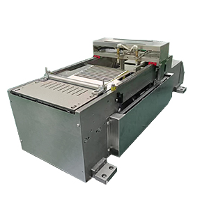
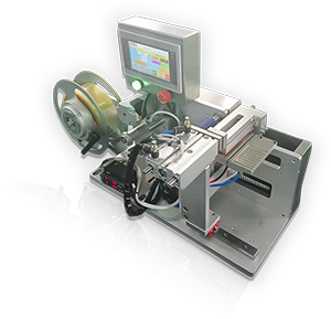
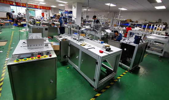
二、视觉贴标机的技术突围路径
LHVT2.0系列设备,通过“三维感知+动态追踪”技术矩阵,构建电子辅材贴合的精度护城河:
1. 微米级视觉定位系统
- 搭载500万像素CMOS相机与10μm级远心镜头,可识别0.02mm²微型标记点
- 采用深度学习算法,对反光/透明材料(如PI膜)的识别准确率达99.7%
- 支持多特征点匹配技术,应对电子辅材的局部形变与位置偏移
2. 动态补偿执行机构
- 直线电机驱动平台实现0.8ms响应速度,动态纠偏精度±0.03mm
- 六轴机械臂柔性适配曲面工件,曲率半径兼容R3mm-R2000mm
- 压力传感贴装头确保辅材零压伤,接触压力控制精度±2g
3. 智能工艺管理系统
- 内置200+电子辅材工艺数据库,一键调用石墨烯膜/电磁屏蔽膜等参数
- 红外热成像模块实时监测贴装温度,防止导热胶因温升发生形变
- 与MES系统深度对接,实现SPC过程管控与质量追溯
三、典型应用场景解析
场景1:微型电子元器件的导电胶贴装
- 痛点:0402封装电阻需在1.0mm×0.5mm区域[敏感词]点胶,人工显微镜操作效率仅15pcs/h
- 解决方案:
① 采用12μm分辨率光学系统捕捉焊盘边界
② 双闭环控制系统实现胶路宽度±0.01mm控制
③ 每小时完成1200件贴装,位置偏移率<0.5‰
场景2:柔性显示屏OCA光学胶贴合
- 痛点:7寸曲面屏贴合气泡发生率超5%,返修造成材料损耗30%
- 创新方案:
① 3D视觉建模技术生成曲面贴合轨迹
② 真空吸附平台消除材料应力形变
③ 在线AOI检测系统实时剔除微米级气泡
④ 良率提升至99.2%,材料利用率提高25%
场景3:动力电池绝缘膜自动化贴覆
- 痛点:电芯表面0.2mm厚蓝膜贴装褶皱导致耐压测试失败
- 技术突破:
① 多光谱检测识别电芯表面凹凸缺陷
② 张力控制系统保持薄膜延展一致性
③ 接触角自适应调整避免边缘翘起
④ 实现0缺陷连续生产8小时
四、行业实证数据
• 某半导体封测企业:导入12台LHVT2.0系列设备,QFN封装散热片贴装CPK值从0.8提升至1.67
• 新能源汽车部件厂商:绝缘板贴标速度达180片/分钟,产线人工成本降低70%
• 消费电子代工厂:TWS耳机导电布贴合良率从82%跃升至98.5%,年节省材料成本超300万元
五、技术演进方向
1. 纳米级精度突破:开发亚微米光学系统,应对第三代半导体材料的贴装需求
2. 多物理场耦合控制:集成温度/湿度/静电防护模块,满足洁净车间特殊工况
3. 数字孪生系统:通过虚拟调试技术将设备导入周期缩短60%
结语
在电子制造向“微米时代”迈进的进程中,龙海环宇“视觉+算法+精密执行”的技术三角,重新定义电子辅材贴合的精度标准。我们诚邀各电子制造企业参与“精度挑战计划”,欢迎免费获取定制化试机方案,共同探索智能制造的新高度。


 微信咨询
微信咨询